various problems cannot be visually inspected after molding
LED
( LED component X-ray Inspection )
For Automotive, ADAS, Smartphone, Electronics application
SEC Co., Ltd / SEC Europe Head Offcie / Automated X-ray Inspection/Nanotech Digital GmbH / Analysis report
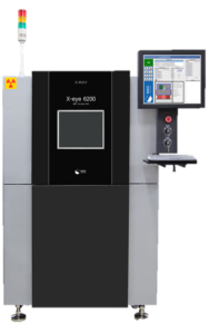
» Analysis systems : by SEC Co.,Ltd
» Inspection method: 2D and 3D
» Model type: Stand-alone
» Model name: X-eye 6200waxi
Wire bonding is the process of creating electrical interconnections between chips and semiconductors or other circuits using bonding wires, which are thin wires made of materials such as gold, silver, copper, and aluminum.
Wire bonding is one of the main processes for connecting signals from LED chips. Defects such as pad peeling, cracking, and delamination affect the development of LEDs, and some of these defects are affected by the wire bonding process.
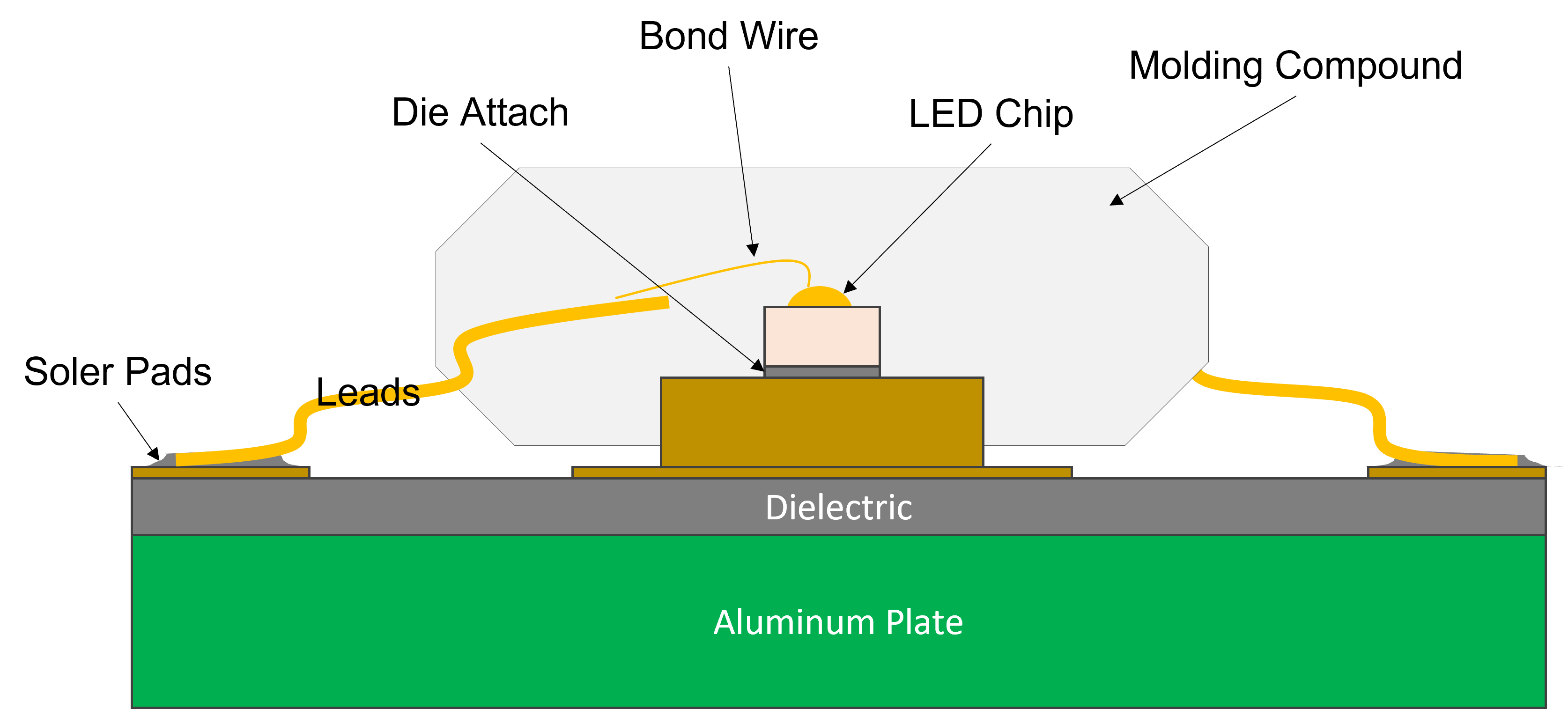
LED Structures
Defects that occur in LEDs can relate to different categories, such as the central element, the chip, and internal and external packaging. A wide range of failures can be inspected due to very different assembly techniques and construction types and different applications.
Because the wire is very thin and stick at high speed so various defects can be inspected.
The types of defects are as follows. Sweep, Broken, Lost, Shift, etc…
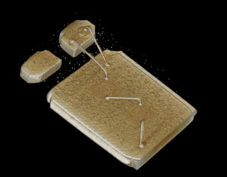
3D LED Wire
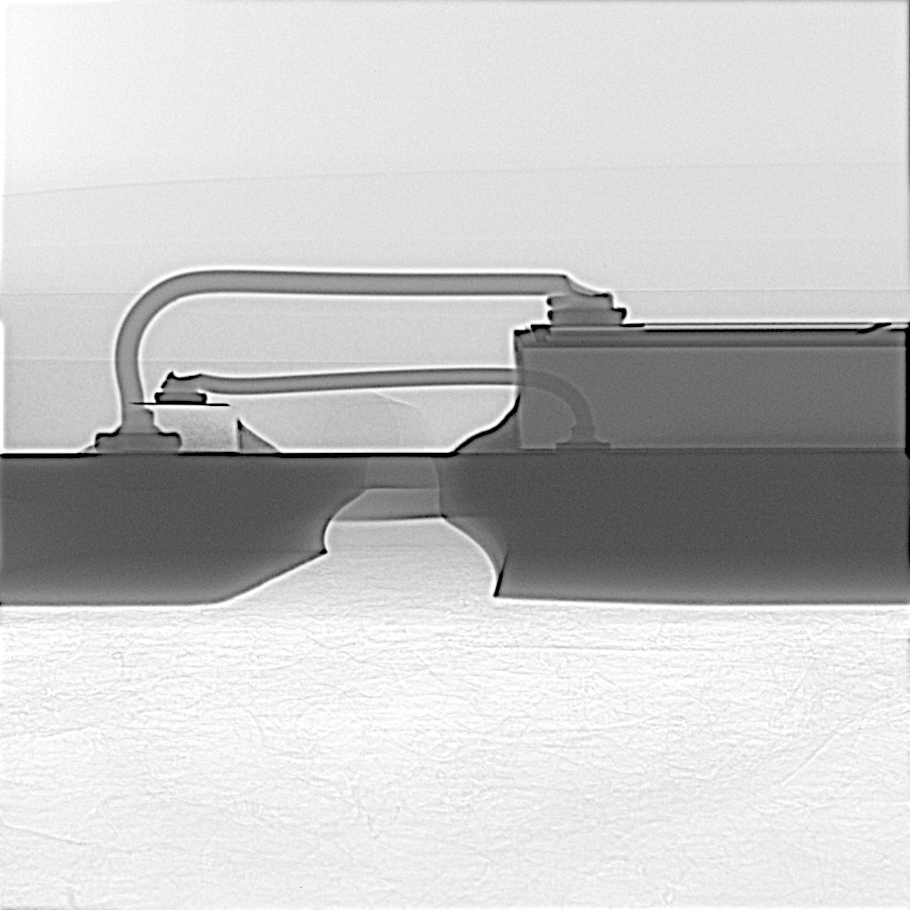
2D LED module
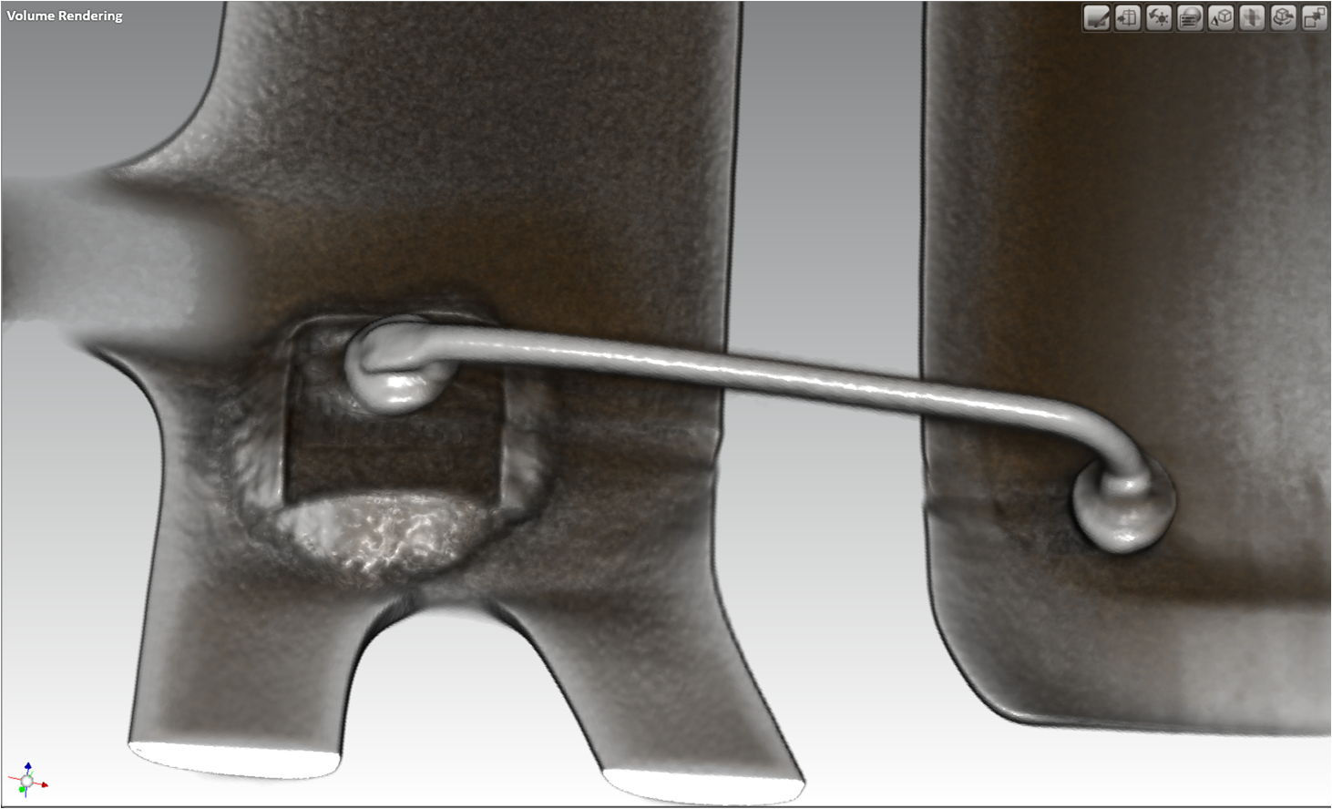
Foreign Material
It can inspect and analyze LED chips through 3D, 2D, and 2.5D to improve quality.
In addition, depending on the type of defect, the process can be modified and complemented, and quality control is possible.
SEC Co., Ltd manufactures X-ray equipment for analysis that enables high-speed inspection and analysis, and inspection of fine wires through 2D, 2.5D, or 3D in One equipment.
