The voids induce many kinds of failure, such as cracks, repeatability, malfunction, reliability, and low electron performance.
Wafer
( Wafer TSV 3D X-ray inspection )
For Semiconductor, Mass production, TSV
SEC Co., Ltd / SEC Europe Head Offcie / Automated X-ray Inspection/Nanotech Digital GmbH / Analysis report
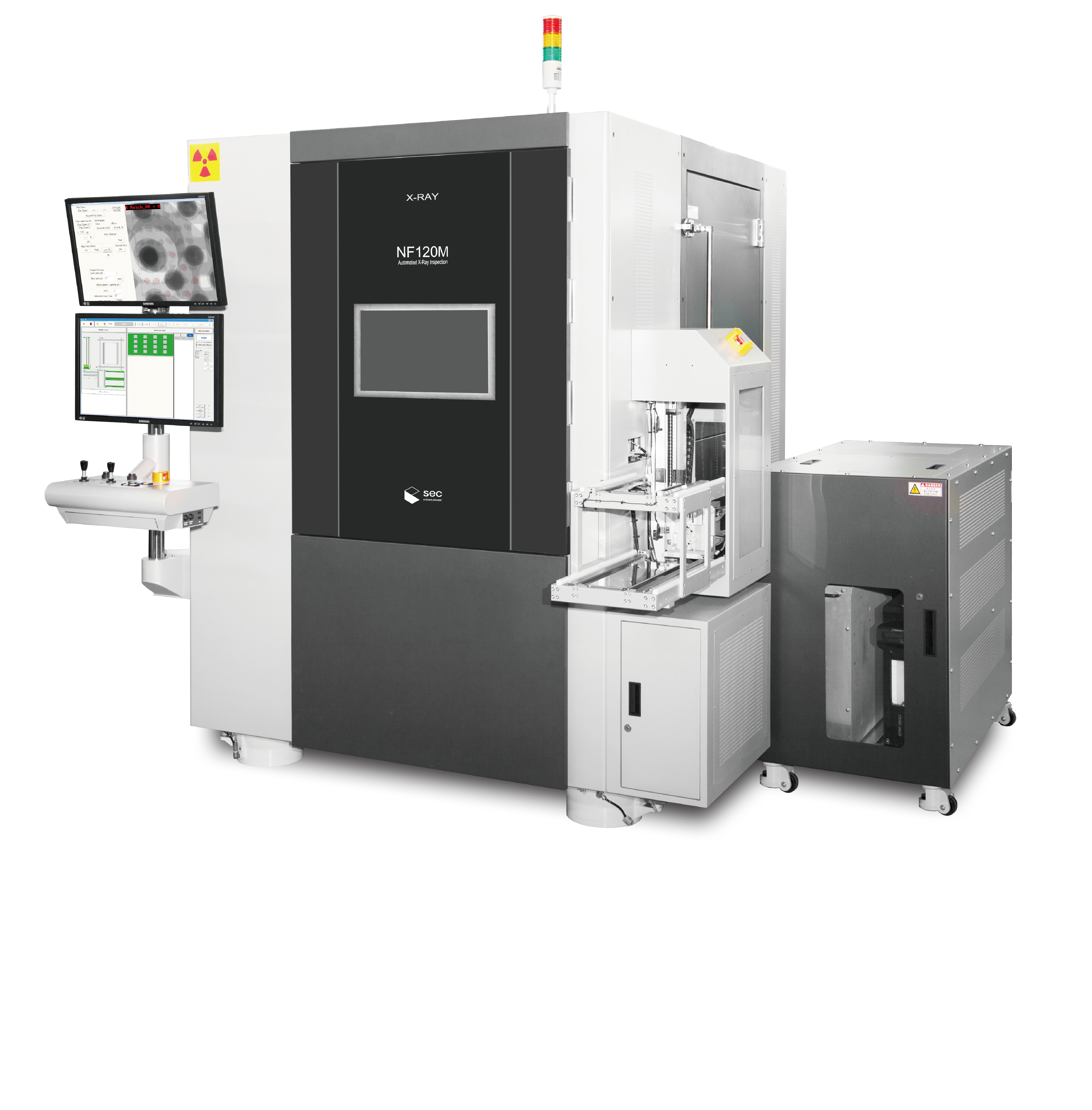
» Analysis systems : by SEC Co.,Ltd
» Inspection method: 2D & 3D
» Model type: Manual & Full-Auto
» Model name: NF120 series
Many dies are made on wafers that have completed semiconductor preprocessing.
In order to use each chip in a field, it is necessary to perform a dicing process of dividing it into individual chips, and then connect external and conductive wires to allow electrons to flow.
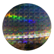
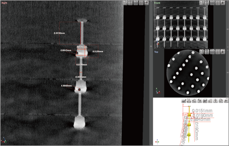
X-ray inspection image of Wafer TSV
TSV is a very important developing that utilises short, vertical connections or via that pass through a wafer in order to establish an electrical connection from the acticated side to backside of the die.
providing the shortest interconnect way and creating an avenue for the ultimate integration.
TSV offers enough space efficiencies and higher interconnect densities than wire bonding and chip stacking.
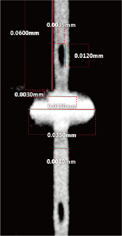
TSV measurement by X-ray inspecton image
TSV have a cylinder with a depth between 10 and 200 μm. The TSV depth is defined by the required thickness during chip or wafer staking, and the aspect ratio is established through the fabrication of the dielectric layer/ barrier/seed/filling process.
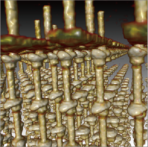
TSV 3D X-ray image
TSV voids are produced during the TSVs fabrication process.
Mainly contains four TSV parts including Cu-filled TSV, void with air, TSV pad, SiO2, and the silicon substrate.
The voids induce many kinds of failure, such as cracks, repeatability, malfunction, reliability, and low electron performance.
X-ray analyses are inspected to guarantee no defects after the process.
