various problems cannot be visually inspected after molding
WAXI
( Wire Automated X-ray Inspection)
For Automotive, ADAS, Smartphone, Camera application
SEC Co., Ltd / SEC Europe Head Offcie / Automated X-ray Inspection/Nanotech Digital GmbH / Analysis report
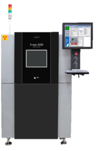
» Analysis systems : by SEC Co.,Ltd
» Inspection method: 2D
» Model type: Full-Auto
» Model name: X-eye 6200waxi
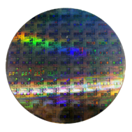
Many dies are made on wafers that have completed semiconductor preprocessing.
In order to use each chip in a field, it is necessary to perform a dicing process of dividing it into individual chips, and then connect external and conductive wires to allow electrons to flow.
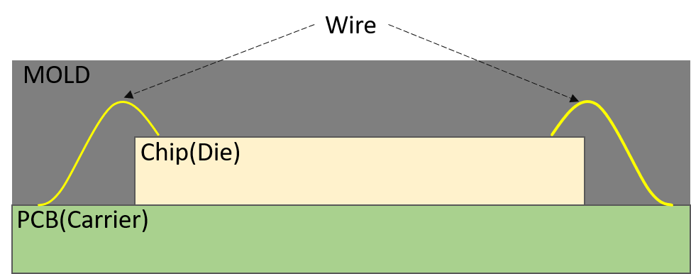
Wire bonding structure
Wire bonding is a method of connecting thin metal wires between a chip and a PCB.
As a technology for connecting the internal chip and the outside, structurally, the wire serves to connect the bonding pad (primary bonding) of the chip and the pad (second bonding) of the carrier.
The material of wire is typically gold (Au), aluminum (Al), and copper (Cu), but gold is mostly used in semiconductor packaging.

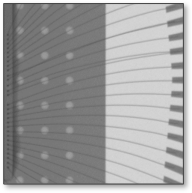
X-ray image of Wire with die
Because the wire is very thin and stick at high speed, various defects occur.
The following problems or other various problems cannot be visually inspected after molding.
X-rays solve these problems.
In addition, quality control is possible through the process of automatically inspecting wires and automatically classifying them.
Overlapped Wire
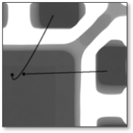
Bending wire
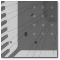
Foreign Material
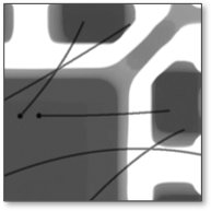
Stray wire
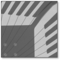
Bent lead
SEC’s software is a self-developed software that sets the test value and proceeds with the test through 4 steps as follows.
1. PKG Unit position teaching
2. Location update to the inpsection software or index Auto wire teaching
3. Overkill & Underkill setting
4. Deep learning training
Automated X-ray Inspection results
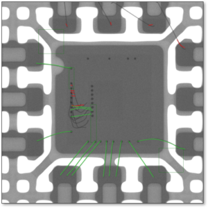
Broken wire
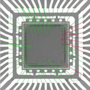
Stray wire
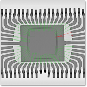
Cross wire
CONTACT
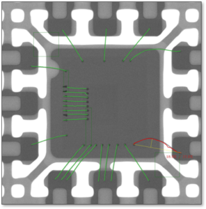
Sweep wire
